Printed circuit boards (PCBs), ICs and IC packages are used in almost all electronic products across all industries: automotive, A&D, consumer electronics, healthcare and energy. With electronics getting smaller, engineers need to design boards that are smaller than ever and incorporate all the required features. Accurate modelling and simulation of these components are key to reliable end products.
- Electrothermal / Electronics Cooling Analysis
- Signal Integrity (SI), Power Integrity (PI) & Electromagnetic Interference (EMI) Analysis
- Shock & Vibration Analysis
- Reliability Prediction
Electrothermal / Electronics Cooling Analysis
ANSYS simulation tools help you manage excessive heat that can otherwise lead to increasing leakage and electromigration failures of the chip, as well as analyse die package, PCB and interconnect thermal differential expansion to enhance reliability of the entire electronic system.
Ansys’ industry leading computational fluid dynamics (CFD) solutions, along with chip-level thermal integrity simulation software, provide all you need to perform electronics cooling simulation and thermal analysis for chip-package, PCB and systems.
The potential for failure in electronic systems due to thermal and mechanical loading of printed circuit boards (PCBs) is escalating due to steadily increasing power dissipation, combined with smaller board sizes. You can conduct thermomechanical stress analysis and airflow analysis to select the ideal heat sink or fan solution that avoids PCB failures due to thermal and mechanical stresses. Ansys’ integrated workflow enables you to conduct design trade-offs, resulting in improved reliability and performance.
Electronics Reliability
Ensuring electronics reliability is a multi-pronged effort, involving selection, optimization and design rules. But, at the end of the day, almost every organization needs a reliability prediction. How long before the product fails and how will it fail? Ansys Sherlock offers specific tools to address these questions.
Signal Integrity
Ansys integrated electromagnetics (EM) and circuit simulation tools predict EMI/EMC, power integrity and SI issues, resulting in optimized system performance prior to build and test.
Design automation features let users:
- Import designs from popular layout tools.
- Perform rigorous electromagnetics extraction.
- Couple to full-circuit simulations.
Many electrical and thermal issues that affect printed circuit boards (PCBs) — electromagnetic interference (EMI), crosstalk, power integrity, overheating, etc. — adversely impact the overall signal integrity of electronic products. These are difficult to predict and expensive to measure. Ansys tools can mitigate signal integrity problems of high-speed digital systems and improve their reliability and performance for first-pass design success.
Power Integrity
For today’s high-speed digital designs, it is critical that printed circuit boards (PCB) and integrated circuit (IC) packages are accurately analysed using a reliable simulation tool like Ansys SIwave so that potential pre- and post-layout power and signal integrity problems are caught early in the design cycles.
Ansys SIwave provides proper verification of power delivery networks for DC power losses, early detection of thermal hotspots, and prevention of failure during the design cycle. It is based on the highest-fidelity electromagnetic numerical analyses to solve all possible aspects involved in the high-speed digital designs of PCBs and IC packages.
Solving DC Power Distribution Problems
 As supply voltages decrease and transistor count follows Moore’s law, DC power delivery is an important consideration for any electronic package or PCB design. Predicting power delivery network (PDN) performance is critical to ensure that a consumer electronic product functions as specified and meets battery life expectations.
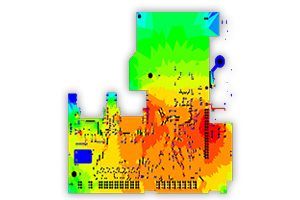
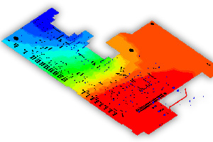
You can predict DC power loss and voltage drop for a package or PCB using the Ansys SIwave-DC simulation tool, then apply those results to improve layout prior to fabrication. As the industry moves toward 3-D IC, it is important to solve complete designs prior to fabrication to prevent system-level failures. Ansys SIwave-DC can extract complete designs (including multiple, arbitrarily shaped power/ground layers, vias, signal traces, wirebonds and circuit elements) with unprecedented accuracy and speed, without requiring manual, often laborious layout partitioning. Multiple layout topologies similar to those in Figure 1 are supported: PoP, SoC, SiP, PKG on PCB.
For the example design, the Vcc power rail supplies 1.8V DC power to two CPUs (U1 and U2). The initial layout brings power from the VRM through an inductor to each of the CPUs. Vcc has only one via transition from layer 1 to layer 5. SIwave-DC finds this problem by highlighting areas of high current and large voltage drops.
Once the problematic area is located, the design engineer can perform simple what-if analyses to determine the best approach for improving the layout. In this example case, the engineer decided to improve the voltage drop by adding a metalized plane at the end of the inductor along; he also added multiple via (10 total) transitions to the power plane located on layer 5. Once the additional metal and via transitions were made, he reran the simulation to determine the impact on the PCB power delivery system.
Ansys SIwave-DC for Power Integrity Analysis
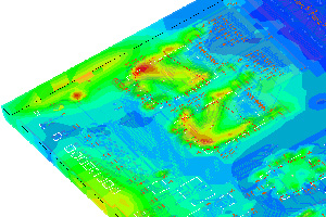
 Hot spots in IC packages can be caused by high current density being drawn by the device in that region. Correct design of power planes and ground planes can help avoid current bottlenecks. Ansys SIwave-DC helps you design current flow pathways and minimize voltage drop across packages and PCBs.
Simulations enable engineers to design PCBs with DC power integrity. It is critical that each of the devices on the board receives reliable power to ensure proper performance. Predictive simulations using Ansys SIwave-DC ensures that the power distribution network can source enough current to ICs on the PCB and into the IC packages. SIwave-DC performs DC analysis of low voltage, high current PCB and IC packages.
Package and Board Power Integrity Design with Ansys SIwave-PI
 Modern design challenges such as 3-D IC and 2.5-D silicon interposers are excellent examples of how we pack more transistors into a smaller form factor. This is also evident from the trends requiring chip-aware system design with increasing transistor density and higher throughput on device IO interfaces. Smaller gate size requires a reduction in gate voltage, thereby shrinking power noise margins. It’s a huge challenge to stay within the shrinking voltage noise limits and keep pace with increasing current demand, since engineers also have to account for signal transitions occurring due to faster edge rates and more transistors switching simultaneously.
While designing PCB systems, the power distribution system plays an integral role in signal transmission. Unless a PCB is designed properly, all of the careful SI and PI engineering on the components and communication links can be wasted. Ansys SIwave offers advanced techniques for full-system power integrity including chip–package–system technologies to provide full coverage for PI simulation needs.
SIwave can extract complete designs (which include multiple, arbitrarily shaped power/ground layers, vias, signal traces, wirebonds and circuit elements) while producing highly accurate models very quickly, without requiring potentially laborious layout partitioning by the user. Multiple layout topologies similar to those in this case study are supported, such as PoP, SoC, SiP and PKG on PCB. Integration of ECAD translation enables simple and seamless geometry translation from popular third-party electrical CAD (ECAD) vendors.
Locations of decoupling capacitors are important in PCDB design; generally, they should be placed close to the DUT, allowing enough room for signal net spacing. SIwave-PI includes PI Advisor, a technology that automates decoupling capacitor selection and placement and optimizes the impedance profile for ECAD. SIwave’s capacitor library browser contains over 20,000 capacitor and inductor models from the industry. It is very useful for evaluating lumped capacitor values with mounting inductance and resistance, viewing multiple impedance curves, and calculating their parallel impedance with easy user-defined filtering features to narrow down capacitor selection. Users can create their own user-defined library of capacitors, inductors and resistors from SPICE and Touchstone models.
Ansys Software to Consider